- 您现在的位置:买卖IC网 > Sheet目录344 > MR256D08BMA45R (Everspin Technologies Inc)IC MRAM 256KB 45NS 48BGA
MR256D08B
2. ELECTRICAL SPECIFICATIONS
Absolute Maximum Ratings
This device contains circuitry to protect the inputs against damage caused by high static voltages or
electric fields; however, it is advised that normal precautions be taken to avoid application of any
voltage greater than maximum rated voltages to these high-impedance (Hi-Z) circuits.
The device also contains protection against external magnetic fields. Precautions should be taken
to avoid application of any magnetic field more intense than the maximum field intensity specified
in the maximum ratings.
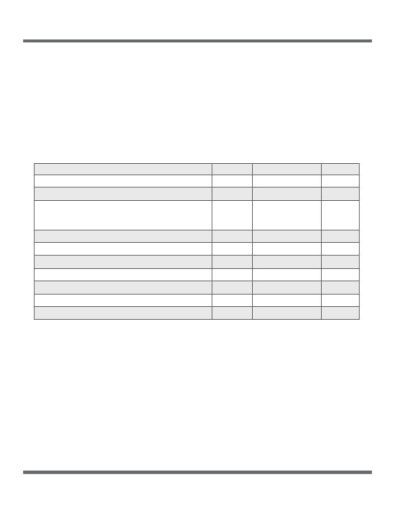
Table 2.1 Absolute Maximum Ratings 1
Parameter
Core Supply voltage 2
I/O Power Supply voltage 2
Symbol
V DD
V DDQ
Value
-0.5 to 4.0
-0.5 to 4.0
Unit
V
V
Voltage on any pin
2
V IN
-0.5 to +4.0 or
V DDQ + 0.5
whichever is less
V
Output current per pin
Package power dissipation 3
Temperature under bias
Storage Temperature
Lead temperature during solder (3 minute max)
Maximum magnetic field during write
Maximum magnetic field during read or standby
I OUT
P D
T BIAS
T stg
T Lead
H max_write
H max_read
±20
0.600
-10 to 85
-55 to 150
260
2000
8000
mA
W
°C
°C
°C
A/m
A/m
Permanent device damage may occur if absolute maximum ratings are exceeded. Functional opera-
All voltages are referenced to V SS .
Power dissipation capability depends on package characteristics and use environment.
1
tion should be restricted to recommended operating conditions. Exposure to excessive voltages or
magnetic fields could affect device reliability.
2
3
Everspin Technologies ? 2011
4
MR256D08B Rev. 3, 12/2011
发布紧急采购,3分钟左右您将得到回复。
相关PDF资料
MR25H10CDF
IC MRAM 1MBIT 40MHZ 8DFN
MR25H256CDF
IC MRAM 256KBIT 40MHZ 8DFN
MR25H40CDF
IC MRAM 4MBIT 40MHZ 8DFN
MR2A08AMYS35R
IC MRAM 4MBIT 35NS 44TSOP
MR2A16ATS35CR
IC MRAM 4MBIT 35NS 44TSOP
MR2A16AVMA35R
IC MRAM 4MBIT 35NS 48BGA
MR4A08BCYS35R
IC MRAM 16MBIT 35NS 44TSOP
MRJ-5385-01
CONN RCPT 8POS 2GRN 1PORT PCB
相关代理商/技术参数
MR256DL08BMA45
功能描述:IC MRAM 256KBIT 45NS 48FBGA 制造商:everspin technologies inc. 系列:- 包装:托盘 零件状态:有效 格式 - 存储器:RAM 存储器类型:MRAM(磁阻 RAM) 存储容量:256K(32K x 8) 速度:45ns 接口:并联 电压 - 电源:2.7 V ~ 3.6 V 工作温度:0°C ~ 70°C(TA) 封装/外壳:48-LFBGA 供应商器件封装:48-FBGA(8x8) 标准包装:348
MR256DL08BMA45R
功能描述:IC MRAM 256KBIT 45NS 48FBGA 制造商:everspin technologies inc. 系列:- 包装:剪切带(CT) 零件状态:有效 格式 - 存储器:RAM 存储器类型:MRAM(磁阻 RAM) 存储容量:256K(32K x 8) 速度:45ns 接口:并联 电压 - 电源:2.7 V ~ 3.6 V 工作温度:0°C ~ 70°C(TA) 封装/外壳:48-LFBGA 供应商器件封装:48-FBGA(8x8) 标准包装:1
MR25B-100R-F
制造商:RF 功能描述:RESISTOR, METAL FILM, 0.25 W, 1 %, 100 PPM, 100 OHM, THROUGH HOLE MOUNT, BULK 制造商:RF Electronics Inc. 功能描述:RESISTOR, METAL FILM, 0.25 W, 1 %, 100 PPM, 100 OHM, THROUGH HOLE MOUNT, BULK
MR25B-10K0-F
制造商:RFE INTERNATIONAL INC 功能描述:RESISTOR, METAL FILM, 0.25 W, 1 %, 100 PPM, 10K OHM, THROUGH HOLE MOUNT, BULK
MR25B-10K2-F
制造商:RFE International Inc 功能描述:RESISTOR, METAL FILM, 0.25 W, 1 %, 100 PPM, 10200 OHM, THROUGH HOLE MOUNT, BULK
MR25B-1132F
制造商:Topohm 功能描述:RESISTOR, METAL FILM, 0.25 W, 1 %, 100 PPM, 11300 OHM, THROUGH HOLE MOUNT, BULK
MR25B-11K0-F
制造商:RFE International Inc 功能描述:RESISTOR, METAL FILM, 0.25 W, 1 %, 100 PPM, 11000 OHM, THROUGH HOLE MOUNT, BULK
MR25B-13K3-F
制造商:RFE International Inc 功能描述:RESISTOR, METAL FILM, 0.25 W, 1 %, 100 PPM, 13300 OHM, THROUGH HOLE MOUNT, BULK
